PCS general secretary FRAN HEATHCOTE explains why opposing war is inseparable from defending jobs, wages and public services – and why readers should come to the London Peace Conference on Saturday June 20

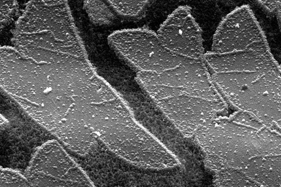
2D or Not 2D: Crystals that open up New Dimensions
Scientists invent a deceptively simple way to build a helter-skelter of atoms

As protests erupt over Henry Nowak’s murder, ANDREW MURRAY argues that anger is being exploited to advance a wider racist and anti-immigration agenda
CARLOS MARTINEZ explains the sound case for car manufacturing co-operation with China
The National Emergency Briefing outlines the need for urgent action to address environmental crisis, says PAUL DONOVAN, warning that there’s no time to indulge the arguments of the fossil-fuel-funded climate-change deniers
Campaigners say criticism of Labour MP Stephen Morgan’s position on Gaza has been met with police intervention and cancelled opportunities for debate. HESTER WOLFE reports
The Committee for the Defence of Iranian People’s Rights warns of escalation danger in Iran war


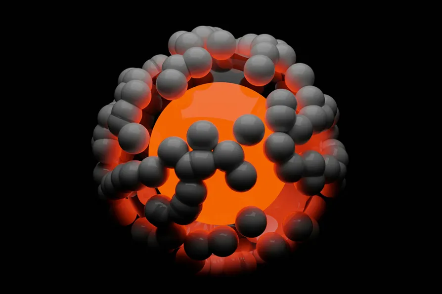
EVERYTHING is made of atoms. To understand this, we’re asked to imagine that the smooth continuous materials around us are each made up of tiny lumps.
Rather than acting like little inert building bricks, each is humming with the energy of existing. Every atom is itself an immense void with even tinier positive and negative charged matter suspended in space, whizzing round each other and changing configuration to give the atom its own particular properties.
The dynamism of the charges moving around and interacting both inside the atom and outside of it defines the ways that charge and energy can move between them, through space, sometimes joining them together in configurations of molecules of infinite variety.

Similar stories

MIRANDA RICHMOND relishes the gloriously liberated art of Roy Oxlade, and traces his method back to the thinking of David Bomberg, his acknowledged teacher
Neutrinos are so abundant that 400 trillion pass through your body every second. ROX MIDDLETON, LIAM SHAW and MIRIAM GAUNTLETT explain how scientists are seeking to know more about them
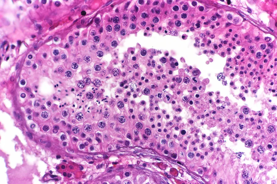
New research into mutations in sperm helps us better understand why they occur, while debunking a few myths in the process, write ROX MIDDLETON, LIAM SHAW and MIRIAM GAUNTLETT

Olive oil remains a vital foundation of food, agriculture and society, storing power in the bonds of solidarity. Though Palestinians are under attack, they continue to press forward write ROX MIDDLETON, LIAM SHAW and MIRIAM GAUNTLETT